- 您现在的位置:买卖IC网 > Sheet目录328 > IDT70T3519S133DRI (IDT, Integrated Device Technology Inc)IC SRAM 9MBIT 133MHZ 208QFP
�� �
�
�SYNCHRONOUS�
�True� Dual-Port� memory� cells� which� allow� simultaneous� Interrupt� and� Collision� Detection� Flags�
�HIGH-SPEED� 2.5V�
�256/128/64K� x� 36�
�IDT70T3519/99/89S�
�DUAL-PORT� STATIC� RAM�
�WITH� 3.3V� OR� 2.5V� INTERFACE�
�Features:�
�◆� ◆�
�access� of� the� same� memory� location�
�◆�
�Separate� byte� controls� for� multiplexed� bus� and� bus�
�◆�
�High-speed� data� access�
�matching� compatibility�
�–� Commercial:� 3.4� (200MHz)/3.6ns� (166MHz)/�
�4.2ns� (133MHz)(max.)�
�–� Industrial:� 3.6ns� (166MHz)/4.2ns� (133MHz)� (max.)�
�◆�
�◆�
�◆�
�Dual� Cycle� Deselect� (DCD)� for� Pipelined� Output� Mode�
�2.5V� (±100mV)� power� supply� for� core�
�LVTTL� compatible,� selectable� 3.3V� (±150mV)� or� 2.5V�
�◆�
�◆�
�Selectable� Pipelined� or� Flow-Through� output� mode�
�Counter� enable� and� repeat� features�
�(±100mV)� power� supply� for� I/Os� and� control� signals� on�
�each� port�
�◆�
�◆�
�Dual� chip� enables� allow� for� depth� expansion� without�
�additional� logic�
�Full� synchronous� operation� on� both� ports�
�–� 5ns� cycle� time,� 200MHz� operation� (14Gbps� bandwidth)�
�–� Fast� 3.4ns� clock� to� data� out�
�–� 1.5ns� setup� to� clock� and� 0.5ns� hold� on� all� control,� data,� and�
�address� inputs� @� 200MHz�
�–� Data� input,� address,� byte� enable� and� control� registers�
�–� Self-timed� write� allows� fast� cycle� time�
�◆�
�◆�
�◆�
�◆�
�◆�
�Industrial� temperature� range� (-40°C� to� +85°C)� is�
�available� at� 166MHz� and� 133MHz�
�Available� in� a� 256-pin� Ball� Grid� Array� (BGA),� a� 208-pin�
�Plastic� Quad� Flatpack� (PQFP)� and� 208-pin� fine� pitch� Ball�
�Grid� Array� (fpBGA)�
�Supports� JTAG� features� compliant� with� IEEE� 1149.1�
�Due� to� limited� pin� count� JTAG� is� not� supported� on� the� 208-�
�pin� PQFP� package�
�Green� parts� available,� see� ordering� information�
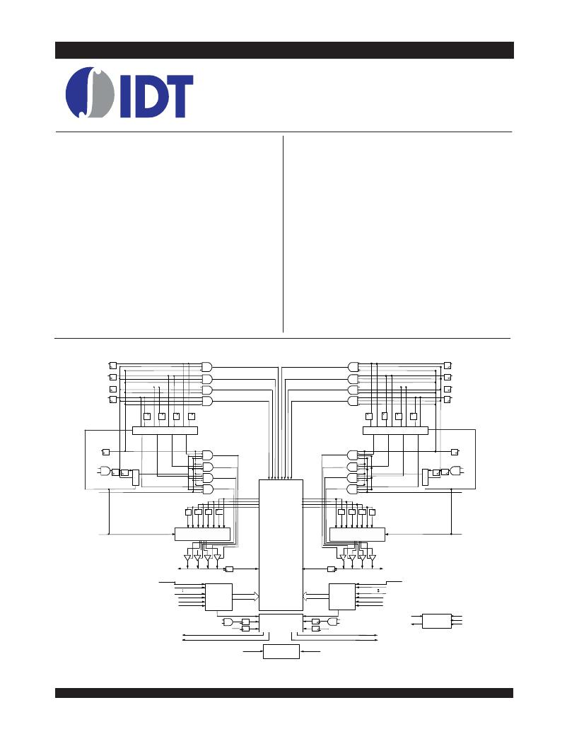
�Functional� Block� Diagram�
�BE� 3L�
�BE� 2L�
�BE� 1L�
�BE� 0L�
�BE� 3R�
�BE� 2R�
�BE� 1R�
�BE� 0R�
�FT� /PIPE� L�
�1/0�
�0a� 1a�
�0b� 1b�
�0c� 1c�
�0d� 1d�
�1d� 0d�
�1c� 0c�
�1b� 0b�
�1a� 0a�
�1/0�
�FT� /PIPE� R�
�a�
�b�
�c�
�d�
�d�
�c�
�b�
�a�
�R/� W� L�
�CE� 0L�
�R/� W� R�
�CE� 0R�
�CE� 1L�
�1�
�0�
�1/0�
�B� B� B� B� B� B� B� B�
�W� W� W� W� W� W� W� W�
�1�
�0�
�1/0�
�CE� 1R�
�0� 1� 2� 3� 3� 2� 1� 0�
�OE� L�
�1d� 0d� 1c� 0c� 1b� 0b� 1a� 0a�
�L� L� L� L� R� R� R� R�
�Dout0-8_L�
�Dout0-8_R�
�Dout9-17_L�
�Dout9-17_R�
�Dout18-26_L�
�Dout18-26_R�
�Dout27-35_L�
�Dout27-35_R�
�0a� 1a� 0b� 1b� 0c� 1c� 0d� 1d�
�OE� R�
�,�
�FT� /PIPE� L�
�0/1�
�abc� d�
�d� cba�
�0/1�
�FT� /PIPE� R�
�256/128/64K� x� 36�
�MEMORY�
�ARRAY�
�I/O� 0L� -� I/O� 35L�
�CLK� L�
�A� 17L(1)�
�Din_L�
�Din_R�
�I/O� 0R� -� I/O� 35R�
�CLK� R�
�A� 17R(1)�
�,�
�A� 0L�
�REPEAT� L�
�ADS� L�
�CNTEN� L�
�Counter/�
�Address�
�Reg.�
�ADDR_L�
�ADDR_R�
�Counter/�
�Address�
�Reg.�
�A� 0R�
�REPEAT� R�
�ADS� R�
�CNTEN� R�
�CE� 0� L�
�CE1L�
�INTERRUPT�
�COLLISION�
�DETECTION�
�CE� 0� R�
�CE1� R�
�TDI�
�TDO�
�JTAG�
�TCK�
�TMS�
�TRST�
�COL� L�
�INT� L�
�R� /� W� L�
�LOGIC�
�R/� W� R�
�COL� R�
�INT� R�
�ZZ� L�
�NOTES:�
�(2)�
�ZZ�
�CONTROL�
�LOGIC�
�ZZ� R�
�(2)�
�5666� drw� 01�
�1.� Address� A� 17� is� a� NC� for� the� IDT70T3599.� Also,� Addresses� A� 17� and� A� 16� are� NC's� for� the� IDT70T3589.�
�2.� The� sleep� mode� pin� shuts� off� all� dynamic� inputs,� except� JTAG� inputs,� when� asserted.� All� static� inputs,� i.e.,� PL/� FT� x� and� OPTx�
�and� the� sleep� mode� pins� themselves� (ZZx)� are� not� affected� during� sleep� mode.�
�1�
�?2014� Integrated� Device� Technology,� Inc.�
�MARCH� 2014�
�DSC� 5666/11�
�发布紧急采购,3分钟左右您将得到回复。
相关PDF资料
IDT70T3539MS166BCG
IC SRAM 18MBIT 166MHZ 256BGA
IDT70T3719MS166BBG
IC SRAM 18MBIT 166MHZ 324BGA
IDT70T633S10BCI
IC SRAM 9MBIT 10NS 256BGA
IDT70T651S12DRI
IC SRAM 9MBIT 12NS 208QFP
IDT70T653MS12BCI
IC SRAM 18MBIT 12NS 256BGA
IDT70V05L55G
IC SRAM 64KBIT 55NS 68PGA
IDT70V06L55G
IC SRAM 128KBIT 55NS 68PGA
IDT70V07L35G
IC SRAM 256KBIT 35NS 68PGA
相关代理商/技术参数
IDT70T3519S166BC
功能描述:IC SRAM 9MBIT 166MHZ 256BGA RoHS:否 类别:集成电路 (IC) >> 存储器 系列:- 标准包装:3,000 系列:- 格式 - 存储器:EEPROMs - 串行 存储器类型:EEPROM 存储容量:8K (1K x 8) 速度:400kHz 接口:I²C,2 线串口 电源电压:1.7 V ~ 5.5 V 工作温度:-40°C ~ 85°C 封装/外壳:8-SOIC(0.154",3.90mm 宽) 供应商设备封装:8-SOIC 包装:带卷 (TR)
IDT70T3519S166BC8
功能描述:IC SRAM 9MBIT 166MHZ 256BGA RoHS:否 类别:集成电路 (IC) >> 存储器 系列:- 标准包装:3,000 系列:- 格式 - 存储器:EEPROMs - 串行 存储器类型:EEPROM 存储容量:8K (1K x 8) 速度:400kHz 接口:I²C,2 线串口 电源电压:1.7 V ~ 5.5 V 工作温度:-40°C ~ 85°C 封装/外壳:8-SOIC(0.154",3.90mm 宽) 供应商设备封装:8-SOIC 包装:带卷 (TR)
IDT70T3519S166BCGI
制造商:Integrated Device Technology Inc 功能描述:IC SRAM 9MBIT 166MHZ 256CABGA
IDT70T3519S166BCI
功能描述:IC SRAM 9MBIT 166MHZ 256BGA RoHS:否 类别:集成电路 (IC) >> 存储器 系列:- 标准包装:3,000 系列:- 格式 - 存储器:EEPROMs - 串行 存储器类型:EEPROM 存储容量:8K (1K x 8) 速度:400kHz 接口:I²C,2 线串口 电源电压:1.7 V ~ 5.5 V 工作温度:-40°C ~ 85°C 封装/外壳:8-SOIC(0.154",3.90mm 宽) 供应商设备封装:8-SOIC 包装:带卷 (TR)
IDT70T3519S166BCI8
功能描述:IC SRAM 9MBIT 166MHZ 256BGA RoHS:否 类别:集成电路 (IC) >> 存储器 系列:- 标准包装:3,000 系列:- 格式 - 存储器:EEPROMs - 串行 存储器类型:EEPROM 存储容量:8K (1K x 8) 速度:400kHz 接口:I²C,2 线串口 电源电压:1.7 V ~ 5.5 V 工作温度:-40°C ~ 85°C 封装/外壳:8-SOIC(0.154",3.90mm 宽) 供应商设备封装:8-SOIC 包装:带卷 (TR)
IDT70T3519S166BF
功能描述:IC SRAM 9MBIT 166MHZ 208FBGA RoHS:否 类别:集成电路 (IC) >> 存储器 系列:- 标准包装:3,000 系列:- 格式 - 存储器:EEPROMs - 串行 存储器类型:EEPROM 存储容量:8K (1K x 8) 速度:400kHz 接口:I²C,2 线串口 电源电压:1.7 V ~ 5.5 V 工作温度:-40°C ~ 85°C 封装/外壳:8-SOIC(0.154",3.90mm 宽) 供应商设备封装:8-SOIC 包装:带卷 (TR)
IDT70T3519S166BF8
功能描述:IC SRAM 9MBIT 166MHZ 208FBGA RoHS:否 类别:集成电路 (IC) >> 存储器 系列:- 标准包装:3,000 系列:- 格式 - 存储器:EEPROMs - 串行 存储器类型:EEPROM 存储容量:8K (1K x 8) 速度:400kHz 接口:I²C,2 线串口 电源电压:1.7 V ~ 5.5 V 工作温度:-40°C ~ 85°C 封装/外壳:8-SOIC(0.154",3.90mm 宽) 供应商设备封装:8-SOIC 包装:带卷 (TR)
IDT70T3519S166BFG
功能描述:IC SRAM 9MBIT 166MHZ 208FPBGA RoHS:是 类别:集成电路 (IC) >> 存储器 系列:- 标准包装:3,000 系列:- 格式 - 存储器:EEPROMs - 串行 存储器类型:EEPROM 存储容量:8K (1K x 8) 速度:400kHz 接口:I²C,2 线串口 电源电压:1.7 V ~ 5.5 V 工作温度:-40°C ~ 85°C 封装/外壳:8-SOIC(0.154",3.90mm 宽) 供应商设备封装:8-SOIC 包装:带卷 (TR)